
What is 4D NAND?

As technology continues to advance, new kinks and components are being introduced. One of the most recent developments in 4D NAND technology is a type of storage technology that can help increase your device’s performance capability while also providing more space for data. With so many questions about 4D NAND, this blog post will go into depth about what it is and how it works.
The Memory Market

The memory industry has undergone a significant transformation in the past year due to increased consumer demand for better performance. In response, Micron recently announced its NAND flash technology with 232 layers — which is the highest-density product currently available on the market.
Along with this breakthrough, Micron also announced faster interface speeds and higher-quality data paths that enable smaller and denser systems that are designed to expand storage capabilities. Thanks to these developments, the memory industry has seen a surge in competition as more companies can now create cutting-edge products at more affordable prices.
SK Hynix has revealed its advancements in NAND technology, unveiling a 238-layer 4D NAND product as a real solution for customer needs. Cheaper than its predecessors, this new technology from SK Hynix is exceptionally reliable and fast, giving the company a competitive edge in the memory market.
Customers looking for high-performance memory solutions will now have yet another leading option to choose from when considering the most suitable products for their particular needs.
Before we dive into the realm of 4D NAND technology, let’s take a quick look back at its predecessor: 3D NAND.
What Is 3D NAND?
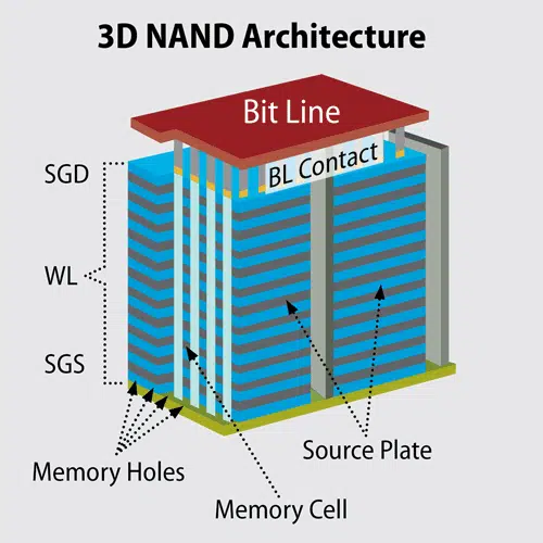
3D NAND is a type of flash memory technology that is used in storage devices such as solid-state drives (SSDs). It is called “3D” because the memory cells are stacked vertically in multiple layers, instead of being arranged in a single plane like in traditional NAND technology. This allows for higher storage capacity, faster data transfer speeds, and improved performance compared to traditional NAND.
3D NAND also offers improved reliability, as it is less prone to failure due to its increased number of memory cells. The technology is used in both consumer-grade storage devices and enterprise-level solutions. With the advancement of 3D NAND, higher capacities and faster speeds are now available for a wide range of applications.
If you want to know more about this technology, take a look at What Is 3D NAND and How Does It Work?
What Is 4D NAND?
4D NAND is a variation of 3D NAND flash technology. In 4D NAND, not only are the memory cells stacked vertically in multiple layers, but the NAND circuitry is also integrated vertically, resulting in higher storage density and improved performance compared to 3D NAND. This technology offers benefits such as increased storage capacity, faster data transfer speeds, and improved energy efficiency.
In traditional 3D NAND technology, the stacked NAND array and peripheral circuitry are separate components. The peripheral circuitry manages memory operations and controls the array. Typically, it is placed beside the 3D NAND array, which takes up valuable die space and restricts the amount of area available for the memory cells.
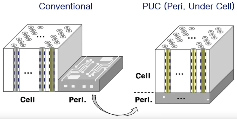
In comparison, 4D NAND integrates the peripheral circuitry underneath the 3D NAND array. This further improves density and reduces costs through vertical integration, similar to 3D NAND.
It is important to note that similar architecture as 4D NAND has been used in the past by companies like Intel and Micron but referred to as “CMOS under Array” (CuA) technology.
CMOS under Array (CuA) technology is an exciting breakthrough in semiconductor chip design. It provides faster speeds, lower costs, and more reliable operation than traditional CMOS chips.
CuA transfers power over the underneath metal layer of an integrated circuit instead of relying on conventional planar metallization values. This revolutionary new approach enables superior performance and scalability with its modern through-silicon-via powering solution.
Compared with traditional CMOS designs, CuA noise margins are significantly improved, and power density when arranged in a compact layout.
SK Hynix’s 4D NAND
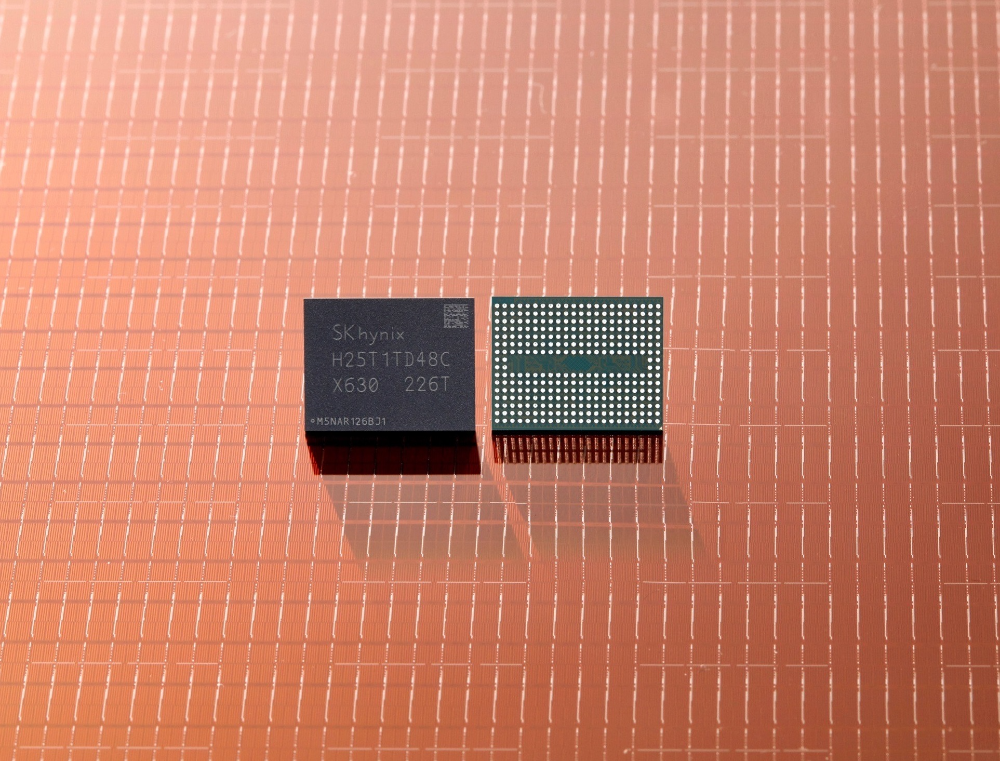
On August 2, SK Hynix announced its new 238-layer 4D NAND technology. The company claims that this new technology is the highest layer-count NAND in the world and has a smaller cell area per unit than other 3D NAND options. This high density leads to improved performance and energy efficiency, with 50% faster data transfer speeds and a 21% decrease in energy consumption compared to their previous 176-layer technology.
SK Hynix has yet to reveal more details, but the press release states that the device has a transfer speed of up to 2.4 Gbps and a memory capacity of 512 Gb. The company intends for its 238-layer product to be used in PC SSDs, with potential future applications in smartphones and server storage. Samples of the product have already been shipped to select customers and mass production is planned to begin in H1 2023.
So far, SK Hynix is the only company to have announced a 4D NAND product, but other industry giants such as Samsung and Intel will likely follow suit soon. With this technology, devices can become more powerful and energy efficient than ever before. Stay tuned for more updates from the leading memory companies!